- 非IC关键词
企业档案
- 相关证件:

- 会员类型:普通会员
- 陈愈柏
- 电话:0755-84664302/84660586-618
- 手机:18923809726
- 地址:龙城街道天安数码城1栋B1003-2
- 传真:0755-84662603
- E-mail:yuhui200808@163.com
您的当前位置:深圳市裕辉美科技有限公司 > 元器件产品
相关产品
产品信息
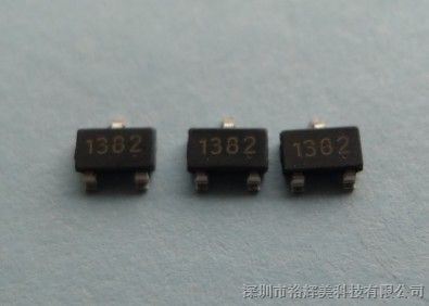
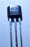
The YH4913s omnipolar Hall effect sensor IC is fabricated from mixed signal
CMOS technology. It incorporates advanced chopper-stabilization techniques to
provide accurate and stable magnetic switch points.
The circuit design provides an internally controlled clocking mechani* to
cycle power to the Hall element and *og signal processing circuits. This serves
to place the high current-consuming portions of the circuit into a Sleep” mode.
Periodically the device is Awakened” by this internal logic and the magnetic flux
from the Hall element is evaluated against the predefined thresholds. If the
flux density is above or below the Bop/Brp thresholds then the output transistor is
driven to change states accordingly. While in the Sleep” cycle the output transistor
is latched in its previous state. The design has been optimized for service in
applications requiring extended operating lifetime in battery powered systems.
The output transistor of the YH4913s will be latched on in the presence of a
sufficiently strong South or North magnetic field facing the marked side of the
package. The output will be latched off in the absence of a magnetic field.
Features
2.2 V to 6.0 V battery operation
High sensitivity and high stability of the magnetic switching points
High resistance to mechanical stress
Di*al output signal
Switching for both poles of a magnet (omnipolar)

